Project Maintainers
Project Contributors

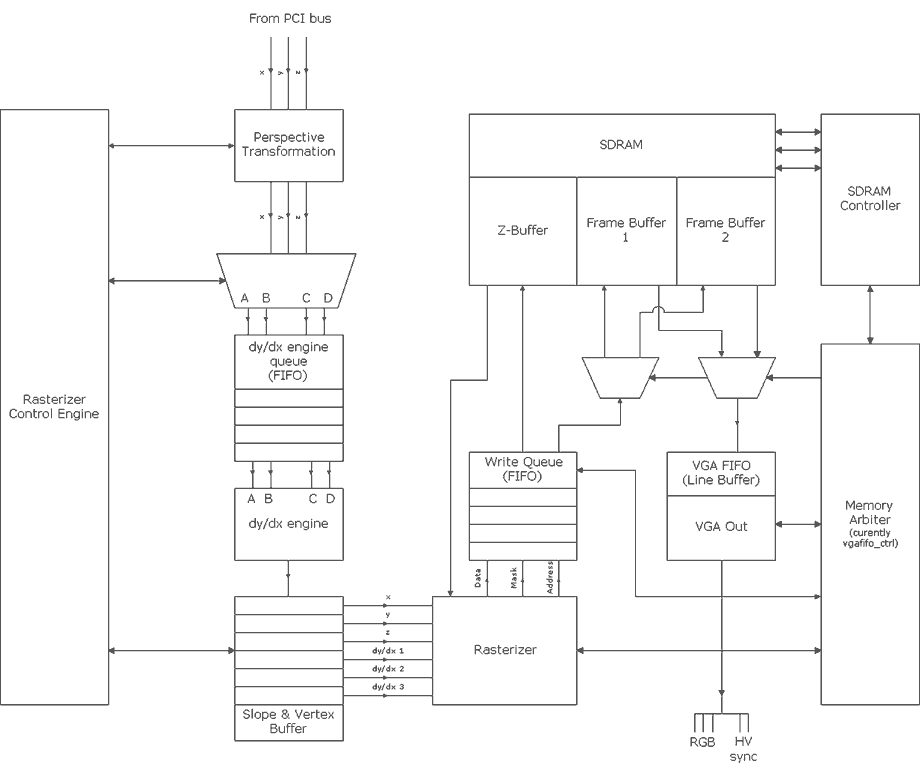
The Manticore processes a triangle and displays it on screen. Triangle information is currently hard-coded, but it will eventually be received over a PCI bus. Triangles are expressed as three <x,y,z> world coordinates. Currently each value is expressed in as 16 bit numbers using a 10.6 fixed point format.
The triangle is transformed for perspective and projected onto the imaging plane, yielding 2D screen coordinates. The slopes of each edge of the triangle are calculated and passed to the rasterizer.
The rasterizer sorts the triangle vertices and calculates which pixels are within the triangle and which are not. For every pixel within the triangle, it writes the triangle's colour to the frame buffer and masks (ignores) all pixels outside of the triangle. It also calculates the z-values of each pixel within the triangle, which will eventually be written to the z-buffer.
The frame buffer is stored in SDRAM. This requires a fully functional SDRAM controller. The frame buffer is read from by the VGA unit, which generates horizontal and vertical sync signals and displays the image on the screen.
Figure 1 shows these steps.
All units are synchronous and have an active low asynchronous reset. The entire design currently operates at 50MHz on an Altera APEX20K200E. The VGA output unit uses a 33MHz pixel clock. The design was originally implemented on a Nios development board, which had a 33MHz clock on board. The built-in PLL on the APEX20KE generates both clocks. If the design is ported to other FPGAs a PLL will be required.
The VGA output module is responsible for displaying the pixels stored in the frame buffer on the screen as well as generating blanking signals. Standard VGA timing for a 640x480 display uses a 25.175MHz pixel clock. Since the Nios board used had a system clock frequency of 33 MHz, non-standard blanking timings were required. For simplicity, the pixel clock frequency is identical to the system clock frequency. The standard 640x480 VGA resolution is also used. A Matrox G400 video card was used to test accurate front porch, sync and back porch timings. The following settings were determined to work with Samsung 900NF, Panasonic E771 and Daytek (unknown model) 17" monitors, although any multisync monitor should tolerate the timings:
| Horizontal refresh: | 40.8 kHz | |
| Active | 640 pixels | 19.17 us |
| Front Porch | 43 pixels | 1.29 us |
| Sync | 46 pixels | 1.38 us |
| Back Porch | 87 pixels | 2.61 us |
| Entire Line | 816 pixels | 24.48 us |
| Vertical refresh: | 76 Hz | |
| Active | 480 lines | 11.75 ms |
| Front Porch | 9 lines | 0.223 ms |
| Sync | 3 lines | 73.44 us |
| Back Porch | 30 lines | 0.734 ms |
| Entire Line | 522 lines | 12.8 ms |
The VGA unit uses 8 bits-per-pixel for colour information, in a 3-3-2 distribution. The VGA unit reads pixel information from a FIFO that buffers an entire line of pixels during the blanking interval. The FIFO begins reading from the frame buffer when the VGA pixel count reaches 640. It continues reading until it buffers an entire line. Since the data width of the SDRAM is 64 bits, the FIFO grabs 8 pixels at a time. The FIFO is emptied as the VGA pixel count increases from 0-639.
The SDRAM controller handles low level SDRAM commands and interfaces with the graphics core.
The SODIMM has a 144-pin interface, which breaks down into clock, clock enable, row address strobe (RAS), column address strobe (CAS), write enable (WE), chip select (CS), a 64-bit data path, a 12-bit address path, and an 8-bit data mask.
RAS, CAS, WE, and CS are all active low signals which specify the RAM command. These commands break down into a row address activation (RAS) followed by one or multiple column address activations (CAS). WE low specifies a write, and WE high specifies a read. Chip select is used to turn on and off the specific chip on the DIMM.
The CAS delay and burst mode of the controller are not generic at this point, but both will be further into development.
The high level interface of the controller consists of a read and write request, and some acknowledge signals. At the moment the acknowledgement signals are being rewritten, so more documentation will be available upon finalization.
A separate module entitled vga_fifo_ctrl handles requests between the graphics core and the SDRAM controller.
The core clock frequency has been reduced to 50MHz because of setup and hold violations with the SDRAM itself. We suspect wiring delays cause this, but the internal controller design could be optimized further.
In order to map 3D triangles onto the display, the perspective transformation is used:
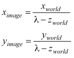
Where λ is the focal length of the imaging system. Since this equation involves two divisions λ was arbitrarily chosen
Once the 2D coordinates are obtained, the slopes of each edge of the triangle are calculated. This operation is performed by the slope calculation engine, which is simply two ALUs and a divider. It is able to calculate arbitrary equations of the form (A +/- B) / (C +/- D). It is also used by the rasterizer to perform slope calculations for each edge of the triangle. The slope of each edge is required by the rasterizer in order to draw arbitrary triangles.
The rasterizer takes the three perspective-corrected vertices and the three slopes and uses an edge-walking algorithm to determine which pixels are within the triangle and which are outside. The algorithm begins at the top of the triangle (i.e. the vertex with the lowest y value) and keeps track of each edge as the y value is increased (towards the bottom of the screen). Since the frame buffer is accessed in bursts of 4 words each and since each word is 8 pixels, every read operation must be aligned to a 4x8 = 32 pixel boundary. Therefore, the rasterization algorithm begins scanning at the nearest 32 pixel boundary to the left of the triangle. As the x value increases, the algorithm checks whether the current pixel is within the triangle or outside. This continues for until the largest y value in the triangle. (Note that the slopes are re-determined when the vertex with the second largest y value is reached.)
Write operations are buffered through a write FIFO. Pixels inside get written to the colour of the triangle and pixels outside have their mask bit set. This permits the overlapping of triangles and other graphics. The write FIFO is emptied during the interval when the memory is idle between read operations.